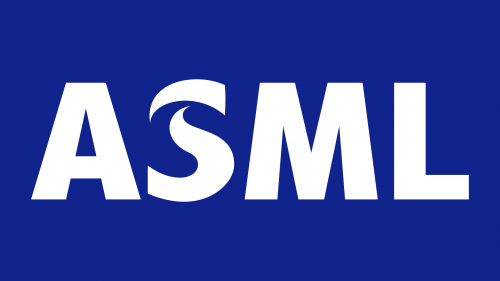
The ASML logo reflects the company’s essence as a leader in high technology. It is the only company worldwide to develop systems for EUV lithography. The minimalist and sleek design emphasizes the high precision essential for patterning silicon wafers in the production of modern microchips.
ASML: Brand overview
ASML was founded in Veldhoven, Netherlands, in 1984. It was a joint venture between Advanced Semiconductor Materials International (ASMI) and Philips, the biggest names in Dutch electronics. ASML stands for “Advanced Semiconductor Materials Lithography.”
The strategic choice was to start the company to create and produce improved lithography systems for the semiconductor sector. At the time, lithography was a crucial technology used in manufacturing integrated circuits, and the founders saw great promise in this area.
When the enterprise started, its primary focus was creating steppers—devices that projected integrated circuit images onto silicon wafers. Initially, the business produced PAS 2000 steppers using technology licensed from Perkin-Elmer, an American company.
1986 was a significant turning point in its history. The PAS 2500 stepper was the firm’s first proprietary product. This gadget marked a major advancement over earlier iterations, and the company entered the race against top producers of lithography equipment.
The firm made significant progress in its growth in 1988 when it established its first foreign office in the United States. This move aimed to improve the company’s standing in the US market and become closer to important Silicon Valley clients.
The first equipment from the business to handle 200mm wafers was the PAS 5000, released in 1991. This noteworthy technological breakthrough strengthened the company’s standing in the market.
Following Philips’ 1995 sale of its ownership interest in the company, the enterprise became independent. The business completed an initial public offering (IPO) on the NASDAQ and Amsterdam stock exchanges the same year, which gave the company the financial means to continue expanding and improving.
For the firm, 1997 was a year of technological innovation. The PAS 5500 was the company’s first step-and-scan system. This technique greatly enhanced the precision and productivity of lithography processes.
Purchasing the Silicon Valley Group’s (SVG) Lithography Systems division in 2000 was a calculated move by the company. With this acquisition, the brand increased its market share in the United States and solidified its position as a leader in technology.
The extreme ultraviolet (EUV) lithography field was first introduced in 2001. The firm committed substantial resources to this exciting technology, which has the potential to transform the semiconductor production industry.
The TWINSCAN XT:1900i is the company’s first immersion lithography system, unveiled in 2007. This technology was a major success at the time because it could attain a resolution of up to 40 nanometers.
A significant advancement in technology occurred in 2010. The company provided the first EUV lithography system prototype. While mass manufacturing was not feasible, this technology showed the firm’s potential for creating cutting-edge lithography solutions.
The Customer Co-Investment Program was introduced in 2012. As part of this initiative, the three biggest investors in the firm, Intel, TSMC, and Samsung, contributed a combined 5.3 billion euros to the company. These expenditures aimed to hasten the advancement of cutting-edge technology such as EUV lithography.
A significant purchase distinguished 2016. For 3.1 billion euros, the firm purchased Hermes Microvision Inc. (HMI), a Taiwanese startup. With the acquisition of HMI, a top producer of electron beam inspection equipment, the company increased the range of products it offers to the semiconductor sector.
In 2018, the enterprise made a significant development in EUV lithography. The business started selling TWINSCAN NXE:3400B EUV lithography systems commercially. With the creation of chips with even greater density and performance, this event signaled the start of a new age in semiconductor manufacturing.
2019 saw record-breaking deliveries for the company. The firm’s delivery of 26 EUV lithography units demonstrated the increased demand for this cutting-edge technology.
In 2020, the company maintained its leadership in cutting-edge lithography technology. The business unveiled the NXE:3400C, a new EUV lithography machine that offered significantly greater precision and performance in producing semiconductors. Chipmakers using this method to miniaturize further and improve microchips’ performance found it a valuable tool.
In 2021, the firm reported major advancements in developing high-NA EUV lithography technology. With a greater numerical aperture than previous generations of EUV systems, this technology paves the way for developing ever smaller and more intricate structures on semiconductor wafers. The company opened a new factory in the Netherlands to fulfill the rising demand for lithography systems, increasing its production capacity.
As of 2022, the company had shipped 100 EUV systems, marking a significant milestone. This accomplishment highlighted the company’s pioneering position in EUV lithography research and commercialization. In addition, the firm unveiled a new sustainability plan that year to lessen its products’ negative environmental effects and raise their energy efficiency.
The company reported that tests of a prototype high-NA EUV system had been successful in 2023, which was a major advancement in developing this technology. By developing relationships with top semiconductor producers in the area and growing its research facility in South Korea, the firm further solidified its position in the Asian market.
The company made large R&D investments to remain the industry leader in lithography technology. Additionally, the enterprise actively addressed the global semiconductor shortage by working with suppliers and customers to enhance supply chain efficiency and optimize production processes.
Meaning and History
What is ASML?
It is a leading Dutch company that supplies advanced semiconductor manufacturing equipment. The company specializes in designing and manufacturing photolithography machines for fabricating integrated circuits (ICs) known as microchips. The brand’s advanced technology enables the production of smaller, faster, and more energy-efficient microchips, playing a crucial role in developing the electronics industry. Major semiconductor manufacturers worldwide use the company’s products, including Intel, Samsung, and TSMC.
1984 – 2012
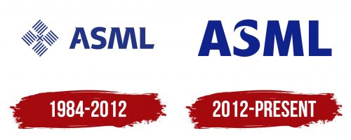
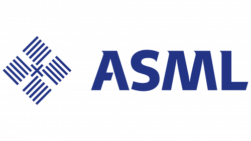
The ASML logo is designed in a minimalist style to emphasize the company’s modernity and innovation. It consists of two parts: an abstract pattern and a brief inscription, which, until 1988, was an abbreviation for Advanced Semiconductor Materials Lithography before becoming the official brand name.
The graphic symbol looks like a diamond composed of four blocks of short lines. They are separated by white negative space in the shape of a cross, with a small letter “X” in the center. This “X” has no particular meaning; it is simply two crossed lines.
The large diamond is a stylized representation of a microchip, aligning with ASML’s primary mission of producing photolithography machines used in chip manufacturing. Their technology enables printing tiny patterns on silicon wafers with precise shape and size control. The emblem mimics the intricate design of an integrated circuit, perfectly reflecting the company’s field of activity.
Next to the striped diamond is the word “ASML,” written in a custom font with short, sharp serifs. Each letter has its specific characteristic:
- The “A” lacks a fragment of the horizontal bar, creating a sense of openness.
- The upper end of the “S” is slightly pointed to match the serifs on the other glyphs.
- The “M” has a relatively wide middle, maintaining a balance between the lines.
- The bottom edge of the “L” is cut diagonally at the same angle as the bar of the “A.”
All serifs are at the top and point only to the left, giving the impression that the inscription is rushing forward at high speed. This illusion of movement indicates the company’s drive to develop new technologies in the semiconductor industry. These nuances make the logo expressive and highlight the innovativeness of the photolithography machine manufacturer. The letters’ consistent stroke thickness and precisely calculated proportions convey a sense of stability and reliability.
The font’s geometric style pairs well with the dark blue color used for both the brand name and the abstract pattern. This color is often associated with high technology, which signifies professionalism, reliability, and stability.
2012 – today
2012, ASML Corporation simplified its logo to align with a minimalist style. As a result, the complex pattern of stripes was removed, leaving only the short, four-letter inscription. Designers combined the wordmark with a new graphic symbol—two wavy lines forming a semblance of an “S.”
The curved shape of the “S” resembles a flow, symbolizing the photolithography process. In this context, the uneven lines represent light waves used in ASML equipment to print images on silicon wafers. The visual movement also conveys continuous development and progress, reflecting the company’s drive for innovation in semiconductor technology.
The rest of the inscription is straightforward, with “A,” “M,” and “L” rendered in a standard bold grotesque font. These letters balance the fluidity of the “S,” making the logo noticeable through contrasting forms. The uniform stroke thickness and the absence of serifs and other decorative elements reflect the high precision essential in photolithography machines.
The uppercase font with clear, straight lines conveys the seriousness and professionalism of ASML. The inscription’s geometric style pairs well with the dark blue color, enhancing the sense of reliability and technological prowess. The chosen palette underscores the company’s innovative nature and achievements in producing advanced equipment.
